Electron Backscatter Diffraction
Electron Backscatter Diffraction (EBSD) is a technique that is uniquely suited to characterize crystallographic properties of your samples. Proprieties such as: grain size, grain shape, grain orientation, grain boundary misorientation, spatial distribution of phases, local deformation and texture can all be characterized by this technique.
EBSD Analysis is a great complement to the excellent capabilities of our X-ray diffraction (XRD) services. While our XRD tools and staff can provide unparalleled information on phase ID, nanocrystalline grain size, thin film thickness and textures; the new capabilities available by EBSD will provide spatial information, help to visualize the microstructure and add to a complete description of your crystalline samples.
Ideal Uses of EBSD
- Visualization of microstructure with spatial coordinates
- Characterization of texture in exact locations such as near welds or on semiconductor bond pads
- Characterization of grain size & texture as it related to finish quality in sheet steel and Al
- Measurement of large grains, without the error associated with LM
- Characterization of special grain boundaries, such as CSL’s and twins
- Measurement of grain misorientation
- Characterization of deformation by examination of intragrain misorientation and grain aspect ratio
- Characterization of epitaxially grown thin films
- Characterization of in-depth texture, by examining cross sections
EBSD Examples
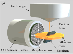
EBSD – Electron Back Scatter Diffraction is a technique using the electron beam of a SEM to differentiate the crystallographic orientations of grains on a sample surface. From EBSD we obtain:
- Grain orientation
- Grain size
- Misorientation between grains
- Pole figures and maps
Strengths
- Accurately provides spatially resolved grain size and phase information from several 10s of nm to several 10s of mm.
- Provides texture information from localized area.
- Provides grain boundary angle information.
- Can be used for failure analysis.
Limitations
- The phase information needs to be known a-priori.
- Cannot analyze amorphous materials.
- Cannot distinguish phases of similar crystal structures (need to use EDS-EBSD technique).
- High-quality polished surface is required.
EBSD Technical Specifications
- Signal Detected: Diffracted electrons
- Elements Detected: All elements, assuming they are present in a crystalline matrix
- Detection Limits: Grain size >80 nm
- Quantitative analysis: Grain size and related measurements: ~10%